Interviews are more than just a Q&A session—they’re a chance to prove your worth. This blog dives into essential Advanced Optics Manufacturing (AOM) Training interview questions and expert tips to help you align your answers with what hiring managers are looking for. Start preparing to shine!
Questions Asked in Advanced Optics Manufacturing (AOM) Training Interview
Q 1. Explain the difference between refractive and diffractive optical elements.
Refractive and diffractive optical elements both manipulate light, but they do so through different mechanisms. Refractive elements, like lenses, bend light by changing its speed as it passes through different refractive index materials. Think of a straw appearing bent in a glass of water – that’s refraction in action. Diffractive elements, on the other hand, use surface structures (like tiny grooves or gratings) to diffract light, essentially creating interference patterns that change the light’s direction. Imagine a CD; the rainbow effect is due to diffraction from the tiny data tracks.
In simpler terms: Refractive elements use material to bend light, while diffractive elements use surface features to bend light. This difference leads to distinct applications. Refractive elements are often used in imaging systems because of their ability to precisely focus light. Diffractive elements are useful in applications like beam shaping or spectral analysis due to their ability to separate light of different wavelengths. For instance, a high-precision refractive lens might be used in a microscope objective, while a diffractive grating is used in a spectrometer to separate the wavelengths of light coming from a star.
Q 2. Describe the process of optical polishing.
Optical polishing is a meticulous process aimed at achieving extremely smooth surfaces on optical components. Imperfections, even at the microscopic level, can significantly impact the performance of an optical system by scattering or distorting light. The process typically involves several stages, starting with rough grinding to shape the component to its desired form. This is followed by progressively finer grinding using abrasives of decreasing particle size. The final step is polishing, which uses very fine abrasives (often pitch or polishing compounds) to remove the remaining scratches and irregularities and achieve an atomically smooth surface.
Imagine smoothing a rock into a perfect sphere. You’d start with a coarse tool, then gradually switch to finer and finer tools until the surface is exceptionally smooth. Optical polishing uses similar principles but with significantly higher precision and control. The quality of the final surface is assessed using techniques like interferometry and surface profilometry, ensuring the component meets stringent specifications.
Q 3. What are common methods for optical coating deposition?
Several methods exist for depositing optical coatings, each with its own advantages and disadvantages. These coatings are crucial for enhancing the performance of optical components, increasing reflectivity, reducing transmission loss, or even creating specialized optical filters. Common methods include:
- Evaporation: Material is heated until it vaporizes, and the vapor condenses onto the optical surface, forming a thin film. This is a relatively simple and cost-effective technique, but it’s less precise in controlling film thickness and uniformity.
- Sputtering: Material is bombarded with ions, causing atoms to be ejected and deposited onto the optical surface. This method is advantageous for creating durable and highly uniform coatings, even on complex shapes.
- Chemical Vapor Deposition (CVD): Precursor gases react on the optical surface, forming a thin film. This technique offers excellent control over film properties, and is often used for creating specialized coatings like anti-reflective coatings.
- Sol-Gel Process: A liquid precursor solution is deposited onto the surface, forming a thin film upon drying and curing. This method is often used for creating porous coatings or coatings with specific chemical properties.
The choice of method depends on factors like the desired coating properties, the complexity of the optical component, and cost considerations. For example, a high-reflectivity mirror might utilize sputtering for its durability, while an anti-reflection coating on a lens might be made using CVD for its precise control of refractive index.
Q 4. How do you measure surface roughness of an optical component?
Surface roughness of an optical component is measured using various techniques that quantify the deviations from an ideal, perfectly smooth surface. The most common methods include:
- Profilometry: This involves scanning the surface with a stylus or optical probe to create a three-dimensional map of the surface profile. This allows for direct measurement of surface roughness parameters such as Ra (average roughness) and Rz (maximum peak-to-valley height).
- Interferometry: By interfering light reflected from the surface with a reference beam, interferometry creates an interference pattern representing the surface’s topography. This technique is highly sensitive and can measure extremely small deviations from flatness, providing high-resolution measurements of surface roughness.
- Scatterometry: This technique measures the amount of light scattered by the surface. The amount of scattering is directly related to the surface roughness. It’s a non-contact method often used for in-line measurements during manufacturing processes.
The choice of method depends on the required precision and the type of optical component. For instance, profilometry might be preferred for measuring relatively rough surfaces, while interferometry is better suited for measuring highly polished surfaces where even minute irregularities are crucial.
Q 5. Explain the principles of interferometry in optical testing.
Interferometry is a powerful technique for optical testing based on the principle of wave interference. When two coherent light waves overlap, they interfere, creating an interference pattern that reveals information about the wavefronts. In optical testing, a reference wavefront (typically from a highly stable laser) is compared to the wavefront reflected or transmitted by the optical component under test. Any deviations from the ideal wavefront, due to imperfections in the component, will result in variations in the interference pattern. These variations can then be analyzed to determine the component’s surface shape, refractive index variations, and other optical properties.
Imagine dropping two pebbles into a still pond. The resulting ripples overlap and create complex interference patterns. Similarly, in interferometry, the interference patterns reveal the subtle variations in the optical component’s surface. Different types of interferometers, such as Fizeau, Twyman-Green, and Mach-Zehnder, are used depending on the specific application and the type of component being tested. For example, a Fizeau interferometer is often used for testing flat surfaces, while a Twyman-Green interferometer is suitable for testing lenses and other curved optical components.
Q 6. What are the key challenges in high-precision optical assembly?
High-precision optical assembly presents several significant challenges due to the extremely tight tolerances required. Even minute errors in alignment or positioning can lead to significant degradation in the performance of the final optical system. Key challenges include:
- Maintaining Alignment Tolerances: Sub-micron alignment precision is often required, necessitating sophisticated assembly techniques and equipment.
- Minimizing Stress and Distortion: Mechanical stress during assembly can induce distortions in the optical components, compromising their performance. Careful selection of materials and assembly methods is crucial.
- Controlling Environmental Factors: Temperature and humidity fluctuations can affect the alignment and performance of optical systems. Environmental control during assembly and operation is often essential.
- Dealing with Complex Geometries: Assembling systems with many components and complex geometries requires careful planning and specialized tooling.
Overcoming these challenges often involves using advanced techniques like active alignment systems, precision micro-positioning stages, and sophisticated environmental control chambers. Furthermore, meticulous planning and design, along with rigorous quality control measures, are essential for successful high-precision optical assembly.
Q 7. Describe different types of optical adhesives and their applications.
Optical adhesives play a crucial role in assembling optical components, providing a means to bond parts without inducing significant stress or optical distortions. Different types of adhesives offer varying properties, making them suitable for different applications:
- UV-curable adhesives: These adhesives cure upon exposure to ultraviolet light, offering rapid curing times and precise control over the curing process. They are often preferred for applications requiring rapid assembly and high precision.
- Epoxy adhesives: Epoxy adhesives offer excellent mechanical strength and chemical resistance, making them suitable for applications where durability and environmental stability are critical. However, they typically require longer curing times.
- Anaerobic adhesives: These adhesives cure in the absence of air, making them useful for bonding components in confined spaces. They are often used in applications where precise control over the bonding area is needed.
- Silicone adhesives: Silicone adhesives offer good flexibility and temperature stability, making them suitable for applications where thermal expansion mismatch between components is a concern.
The choice of adhesive depends on various factors, including the materials being bonded, the required curing time, the environmental conditions, and the desired mechanical and optical properties. For instance, a UV-curable adhesive might be used for assembling a precision optical lens system, while an epoxy adhesive might be used for bonding a large optical mirror to its mount.
Q 8. How do you ensure cleanliness in an optical manufacturing environment?
Maintaining cleanliness in an optical manufacturing environment is paramount because even microscopic particles can severely impact the performance of precision optical components. Think of it like this: a single dust mote on a lens can cause a significant distortion, much like a tiny speck of dirt on a pristine camera lens ruins a photograph. We employ a multi-layered approach:
- Cleanroom Environments: We work primarily within ISO Class 7 or better cleanrooms, utilizing HEPA filtration systems to remove airborne particles. These rooms have controlled temperature and humidity to minimize the risk of condensation or static electricity.
- Personal Protective Equipment (PPE): All personnel wear cleanroom suits, gloves, and face masks to prevent contamination from clothing fibers, skin cells, and hair. Specialized footwear is also required.
- Cleaning Procedures and Materials: We use highly purified solvents and specialized cleaning cloths, often made of lint-free materials. Components are meticulously cleaned using techniques like ultrasonic cleaning or isopropyl alcohol wiping, followed by a thorough drying process using nitrogen gas or clean, dry air. The choice of cleaning method depends on the material and surface of the optical component.
- Regular Cleaning and Inspection: Regular cleaning schedules are rigorously followed, and air quality is constantly monitored. Periodic audits and inspections ensure our cleaning processes are effective and meet industry standards.
- Controlled Material Handling: Components are handled with specialized tools, and transported in clean containers to prevent contamination throughout the manufacturing process.
Failing to maintain this stringent level of cleanliness would result in unacceptable levels of scattering, absorption, and surface defects, ultimately rendering the optical components unusable.
Q 9. Explain the concept of optical tolerancing.
Optical tolerancing defines the acceptable range of deviations from the ideal design specifications for optical components and systems. It’s essentially setting the limits for how much imperfection is acceptable before the performance of the optical system is negatively impacted. Think of it like building a house – you need to allow for small variations in the dimensions of the bricks, or the doors won’t fit properly. But the variations must be within tolerable limits; otherwise the structure will be unstable.
Optical tolerancing involves specifying tolerances for various parameters, including:
- Surface figure: How precisely the surface curvature matches the design.
- Surface roughness: The texture of the surface, affecting scattering.
- Center thickness: The thickness of a lens at its center.
- Diameter: The size of the optical component.
- Clear aperture: The usable area of the lens.
- Coating thickness: Affecting reflectivity and transmission.
Tolerances are usually expressed as a range of values (e.g., a lens with a center thickness of 10mm ± 0.1mm). Determining appropriate tolerances involves balancing cost and manufacturing feasibility with the required performance of the final optical system. Advanced tolerance analysis software often simulates the effect of various tolerances to optimize design and manufacturing.
Q 10. What are the common defects found in optical components and how are they detected?
Common defects in optical components can significantly degrade performance. Detecting them early is crucial. Some prevalent defects include:
- Scratches: Surface imperfections caused by abrasion, visible as linear marks.
- Dents/Digs: Localized depressions on the surface.
- Pits: Small, isolated surface defects, similar to very small dents.
- Chipping: Loss of material at the edge or surface of a component.
- Bubbles: Inclusions of gas or other materials within the bulk material.
- Inclusions: Foreign particles embedded within the optical material.
- Striae: Variations in the refractive index within the bulk material, appearing as streaks or lines.
Detection methods vary depending on the type of defect and its severity:
- Visual Inspection: A basic method using magnification tools like microscopes or optical comparators.
- Interferometry: High-precision optical measurement technique for surface figure analysis. It uses interference patterns to detect subtle surface variations.
- Scatterometry: Measures light scattering to characterize surface roughness and defects.
- Transmittance/Reflectance Measurements: Assess the optical properties of the component, identifying defects that affect light transmission or reflection.
Advanced techniques such as X-ray inspection might be used to detect internal defects like bubbles or inclusions.
Q 11. Describe different types of optical materials and their properties.
Optical materials are the heart of any optical system, each possessing unique properties that affect the performance of the final product. The choice of material depends critically on the application’s requirements, such as wavelength range, temperature stability, and mechanical strength. Here are a few examples:
- Glass (e.g., BK7, Fused Silica): The most common optical material, offering good transmittance in the visible and near-infrared regions. Fused silica exhibits excellent thermal and chemical stability, while BK7 is a cost-effective choice. Different glass compositions offer varying refractive indices and Abbe numbers.
- Crystals (e.g., Calcium Fluoride, Zinc Selenide): Used in applications requiring high transmittance in the infrared (IR) spectrum. Crystals often exhibit higher refractive indices and better damage thresholds than glass.
- Polymers (e.g., PMMA, Zeonex): Lightweight and less expensive options, suitable for some applications but typically with lower scratch resistance and less precise optical performance than glass or crystals.
- Semiconductors (e.g., Silicon, Gallium Arsenide): Used in specific applications where their electronic and optical properties are exploited. They often exhibit high refractive indices.
Material selection is often a compromise between cost, performance, and the constraints of the specific application. For example, if high precision and stability over a wide temperature range are needed, fused silica might be chosen, despite its higher cost.
Q 12. What is the significance of Abbe number in optical design?
The Abbe number (νd) is a crucial parameter in optical design, representing a material’s dispersion. Dispersion describes how much the refractive index of a material changes with wavelength. A higher Abbe number indicates lower dispersion. Imagine shining white light through a prism – the higher the dispersion, the more the colors separate.
In optical design, minimizing chromatic aberration is essential. Chromatic aberration is the blurring of an image caused by different wavelengths of light focusing at different points. Materials with higher Abbe numbers contribute to reduced chromatic aberration because their refractive indices vary less with wavelength. This is why in many achromatic lens designs, a combination of materials with different Abbe numbers is used to compensate for the different wavelengths.
For example, in an achromatic doublet lens, a high-dispersion glass (low Abbe number) is combined with a low-dispersion glass (high Abbe number) to correct for chromatic aberration. The appropriate choice of glasses with different Abbe numbers allows the designer to minimize color fringing and achieve a sharper, clearer image.
Q 13. How do you perform alignment and adjustment of optical systems?
Aligning and adjusting optical systems is a precise process requiring careful attention to detail and specialized equipment. The goal is to ensure all optical components are positioned correctly, maximizing performance and minimizing aberrations. The process typically involves:
- Initial Component Placement: Using kinematic mounts, components are carefully positioned based on design specifications.
- Coarse Alignment: Preliminary alignment is often done using visual inspection and simple adjustments of component mounts. Laser sources and screens are commonly used to achieve coarse alignment.
- Fine Alignment: Precision adjustments are made using micrometer screws or other fine-adjustment mechanisms, often guided by interferometric measurements or other precision metrology tools. This step ensures that the components meet the exact specifications.
- Optimization: The system’s performance is carefully evaluated, often using a variety of test methods, including image analysis, spot diagrams, and MTF (modulation transfer function) measurements. Based on these results, minor adjustments are made to optimize performance.
- Locking and Stabilization: Once optimal alignment is achieved, the components and mounts are securely locked to prevent movement or vibration.
Advanced optical alignment techniques, such as autocollimation and laser interferometry, provide highly precise measurements and enable more accurate alignment procedures. Specialized software can simulate the effect of adjustments and provide guidance for achieving optimal performance.
Q 14. Explain the principles of optical scattering.
Optical scattering is the phenomenon where light deviates from its original path upon interacting with a surface or medium. It’s like throwing a ball at a rough surface; instead of bouncing straight back, it scatters in many different directions. In optics, this scattering reduces the amount of light transmitted or reflected in the intended direction, degrading image quality and performance.
Several factors contribute to scattering:
- Surface Roughness: A rough surface scatters more light than a smooth one. Microscopic irregularities on a surface cause light to scatter in various directions.
- Bulk Scattering: Inclusions or inhomogeneities within the optical material itself (like dust, bubbles, or striae) can scatter light.
- Wavelength of Light: The amount of scattering can depend on the wavelength of light. Shorter wavelengths (like blue light) are often scattered more than longer wavelengths.
Consequences of scattering can range from minor image degradation to severe performance issues depending on the application. In high-precision applications, such as telescopes and laser systems, even small amounts of scattering can be problematic, affecting image resolution and contrast. To reduce scattering, careful material selection, surface polishing techniques and high-quality manufacturing practices are implemented.
Q 15. Describe the process of optical component testing and inspection.
Optical component testing and inspection is a crucial process ensuring the quality and performance of optical elements. It involves a series of meticulous measurements and analyses to verify that the components meet specified design parameters and tolerances.
- Visual Inspection: This initial step involves checking for surface scratches, digs, chips, or other physical defects using microscopes or low-power magnification. Think of it like carefully examining a gemstone for imperfections.
- Dimensional Measurements: Precise measurements of component dimensions (diameter, thickness, radius of curvature) are performed using tools like interferometers, CMMs (Coordinate Measuring Machines), and profilometers. Accuracy is paramount here; even tiny deviations can significantly impact performance.
- Optical Performance Testing: This is where the real magic happens. We assess the optical properties, such as:
- Transmission and Reflection: Measuring the amount of light that passes through or reflects off the component. Spectrophotometers are commonly employed, giving a detailed spectral response.
- Scattering: Determining the amount of light scattered by imperfections within the component. Low scattering is crucial for high-quality imaging systems.
- Wavefront Aberrations: Analyzing the distortion introduced by the component on the wavefront of light. Interferometry is the gold standard here, showing deviations from the ideal wavefront as fringe patterns.
- Surface Roughness: Measuring the surface texture at a microscopic level using techniques like atomic force microscopy (AFM) and profilometry. Smoother surfaces contribute to better image quality.
For example, in the manufacturing of high-precision lenses for a telescope, rigorous testing ensures that the lens accurately focuses light, minimizing aberrations and achieving the required resolution. Any deviation from specifications could result in blurry images.
Career Expert Tips:
- Ace those interviews! Prepare effectively by reviewing the Top 50 Most Common Interview Questions on ResumeGemini.
- Navigate your job search with confidence! Explore a wide range of Career Tips on ResumeGemini. Learn about common challenges and recommendations to overcome them.
- Craft the perfect resume! Master the Art of Resume Writing with ResumeGemini’s guide. Showcase your unique qualifications and achievements effectively.
- Don’t miss out on holiday savings! Build your dream resume with ResumeGemini’s ATS optimized templates.
Q 16. What are the safety precautions in handling lasers and optical components?
Laser safety and the safe handling of optical components are paramount in AOM. Lasers emit high-intensity light that can cause serious eye and skin damage. Optical components, especially lenses and mirrors, can focus laser beams, further increasing the risk.
- Eye Protection: Always wear appropriate laser safety eyewear, specifically rated for the laser’s wavelength and power. This is the single most important precaution. Think of it as wearing a helmet when riding a motorcycle – essential for safety.
- Laser Safety Training: Thorough training on laser safety procedures and emergency protocols is non-negotiable. This training covers safe operating procedures, emergency shutdown procedures, and the understanding of laser safety classifications.
- Controlled Environment: Laser operations should always be conducted in a controlled environment, minimizing reflections and scattering of laser beams. This includes using beam stops, baffles, and enclosures.
- Proper Handling of Components: Optical components are delicate and should be handled with care to avoid scratching or damaging their surfaces. Use clean gloves and lint-free cloths. Cleanliness prevents scattering and improves performance.
- Emergency Procedures: Clear emergency procedures, including the location of eye wash stations and first-aid kits, must be readily available and understood by all personnel.
Ignoring these safety precautions can lead to severe consequences, from eye damage and burns to potentially lethal accidents. A strict adherence to safety protocols is not just a best practice but a legal requirement in most jurisdictions.
Q 17. Explain the principles of thin-film interference.
Thin-film interference is a phenomenon that occurs when light reflects from the top and bottom surfaces of a thin transparent film. The interference between these reflected waves leads to constructive or destructive interference, resulting in enhanced or suppressed reflection at certain wavelengths. Think of it like ripples in water interfering with each other.
The condition for constructive interference (bright reflection) is given by:
2 * n * d * cos(θ) = m * λwhere:
nis the refractive index of the filmdis the thickness of the filmθis the angle of incidencemis an integer (order of interference)λis the wavelength of light
Destructive interference (low reflection) occurs when the path difference is an odd multiple of half the wavelength. This principle is exploited in the design of anti-reflection coatings, where a thin film with a carefully chosen refractive index and thickness is deposited on a lens surface to minimize reflection and maximize transmission. Conversely, high-reflection coatings utilize constructive interference to maximize reflection at specific wavelengths. Examples include anti-reflection coatings on eyeglasses and high-reflection coatings on mirrors used in lasers.
Q 18. How do you troubleshoot issues in an optical manufacturing process?
Troubleshooting in optical manufacturing requires a systematic approach. It’s akin to detective work, piecing together clues to pinpoint the root cause.
- Identify the Problem: Clearly define the issue. Is it low yield, poor surface quality, or performance degradation?
- Gather Data: Collect relevant data from various sources, such as process parameters, inspection results, and historical records. This might involve reviewing process logs, examining rejected components, or conducting additional tests.
- Analyze Data: Examine the data to identify patterns and potential correlations. Are certain parameters consistently outside tolerance? Are there commonalities among rejected components?
- Formulate Hypotheses: Develop potential explanations based on the data analysis. Consider possible causes, such as issues with the raw materials, process equipment, or operator technique.
- Test Hypotheses: Design and conduct experiments to validate or refute the hypotheses. This may involve adjusting process parameters, replacing components, or conducting controlled tests.
- Implement Corrective Actions: Once the root cause is identified and verified, implement corrective actions to address the problem. This may involve modifying the process, retraining operators, or upgrading equipment.
- Monitor Results: Monitor the process after implementing corrective actions to ensure that the problem has been resolved and that the process is stable.
For example, if consistently low transmission is observed in a batch of lenses, we might hypothesize that there is an issue with the anti-reflection coating deposition process. We would then systematically check the coating parameters, the cleanliness of the chamber, and the quality of the coating materials.
Q 19. Describe your experience with optical metrology equipment.
My experience with optical metrology equipment is extensive. I’m proficient in operating and interpreting data from various instruments, including interferometers (Fizeau, Twyman-Green, and Mach-Zehnder), profilometers (white-light, confocal), scatterometers, and ellipsometers. I’ve used these tools to characterize various optical components, from simple lenses and mirrors to complex freeform optics.
For example, I’ve used a Zygo interferometer to measure the surface figure and roughness of large-diameter mirrors, achieving sub-nanometer accuracy. I’ve also used a white-light profilometer to characterize the surface topography of micro-optical components. My experience extends beyond the simple operation; I understand the underlying principles and limitations of these instruments, which allows me to select the appropriate technique for a given measurement task and interpret the results accurately.
Furthermore, I’m skilled in data analysis techniques using software associated with these instruments, ensuring accurate quantification and interpretation of measurements. This ability to accurately interpret data is crucial for identifying areas needing improvement during the manufacturing process.
Q 20. What software packages are you familiar with for optical design and analysis?
I’m proficient in several optical design and analysis software packages, including Zemax, Code V, and LightTools. My experience encompasses the full design cycle, from initial conceptualization and ray tracing to tolerancing and optimization.
In Zemax, for instance, I can create and analyze complex optical systems, optimizing performance for various parameters like image quality, spot size, and throughput. I can also use these tools to simulate manufacturing tolerances and predict the impact on system performance. Code V is useful for more rigorous analysis of aberration and diffraction effects, whilst LightTools is excellent for non-sequential ray tracing, useful for systems with complex geometries or scattering.
Beyond the specific software, I possess a strong theoretical understanding of optical design principles, which enables me to effectively utilize these tools and interpret the results obtained. This understanding helps in selecting the optimal simulation method for a specific application.
Q 21. Explain your experience with different optical fabrication techniques.
My experience with optical fabrication techniques encompasses a wide range of methods, including:
- Precision Grinding and Polishing: I’m well-versed in the techniques used to shape optical components to the required surface accuracy and finish, utilizing different abrasive materials and polishing compounds. This includes understanding the relationship between the abrasive and the polishing process for achieving different surface finishes.
- Thin-Film Deposition: I’m experienced in various thin-film deposition techniques such as physical vapor deposition (PVD) and chemical vapor deposition (CVD) and understand the importance of controlling deposition parameters for achieving desired optical properties, such as anti-reflection or high-reflection coatings.
- Diamond Turning: I’ve worked with diamond turning for the fabrication of aspheric and freeform optics, understanding the importance of machine parameters and toolpath optimization to achieve high-precision surface figures. This high-precision technique requires specialized machines and expertise.
- Optical Bonding: I’m proficient in various optical bonding techniques, ensuring precise alignment and minimal stress. This is crucial for assembling complex optical systems.
I understand the strengths and limitations of each technique and can select the most appropriate method for a given component and specification. Moreover, I’m familiar with quality control procedures at each stage of the fabrication process to ensure the final product meets the required performance specifications.
Q 22. How do you ensure the quality and reproducibility of optical manufacturing processes?
Ensuring quality and reproducibility in optical manufacturing is paramount. It involves a multi-faceted approach encompassing meticulous process control, rigorous quality checks, and proactive preventative measures. Think of it like baking a cake – you need precise ingredients, the right temperature, and the correct baking time to get a consistently delicious result.
- Process Parameter Control: We utilize sophisticated equipment with automated control systems to maintain precise parameters like temperature, pressure, and humidity during processes like polishing, coating, and cleaning. Slight variations can drastically impact the final product’s quality.
- Regular Calibration and Maintenance: All equipment undergoes scheduled calibration and preventative maintenance to ensure accuracy and consistent performance. This minimizes the risk of errors and ensures consistent results over time.
- In-Process Quality Control: We implement multiple checkpoints during the manufacturing process where samples are inspected to identify and correct any deviations from specifications early on, preventing defects from propagating through the entire production line. This ‘early detection’ is crucial.
- Material Traceability: Maintaining a comprehensive record of all materials used, including their source, batch number, and quality certifications, ensures that we can trace the origin of any potential issue, allowing for rapid identification and correction.
- Documentation and Standard Operating Procedures (SOPs): We adhere to strictly defined SOPs for every step of the process, meticulously documenting all procedures and findings. This ensures consistency across batches and allows for easy troubleshooting and improvements.
By implementing these strategies, we minimize variations and ensure the consistent production of high-quality optical components.
Q 23. Describe your understanding of statistical process control (SPC) in optical manufacturing.
Statistical Process Control (SPC) is essential in optical manufacturing for monitoring and controlling process variations. Imagine it as a ‘watchdog’ for our manufacturing process, constantly observing for any signs of trouble. We use control charts, such as X-bar and R charts, to track key process parameters (like surface roughness or refractive index) over time. These charts help us identify trends, shifts, or patterns in the data which might indicate a problem before it significantly impacts the product quality.
For example, if the average surface roughness consistently exceeds the upper control limit, it suggests a problem with the polishing process requiring investigation. We may need to check the polishing pad condition, adjust the polishing slurry, or even recalibrate the polishing machine. SPC allows for proactive interventions, preventing the production of faulty components and minimizing waste.
Beyond the basic control charts, we also employ more advanced SPC techniques like process capability analysis (Cpk) to determine the process’s ability to consistently meet customer specifications. This ensures we can confidently deliver products within the required tolerances.
Q 24. Explain your experience with different types of optical sensors.
My experience encompasses a range of optical sensors critical for different stages of advanced optics manufacturing. Think of these sensors as the ‘eyes’ of our manufacturing process, providing crucial feedback on the quality and precision of our work.
- Interferometers: These are indispensable for measuring surface shape and figuring accuracy, especially in precision optics like lenses and mirrors. We use Fizeau and Twyman-Green interferometers to analyze wavefront errors down to nanometers.
- Optical Profilometers: These sensors are invaluable for measuring surface roughness and topography, providing crucial information on the quality of polishing and coating processes. Examples include confocal and white-light interferometry systems.
- Spectrometers: Used extensively in thin-film coating processes, spectrometers measure the reflectance and transmittance of optical coatings, ensuring their spectral properties meet the required specifications.
- Power Meters: For laser-based processes, we employ power meters for precise control and monitoring of laser power and beam profile.
- Scatterometers: These help analyze surface roughness and defects at the nanoscale, providing detailed information about the quality of the optical surface.
My experience includes operating, calibrating, and troubleshooting a variety of these sensors to ensure accurate and reliable measurements are obtained.
Q 25. What are the key performance indicators (KPIs) you would use to evaluate the performance of an optical manufacturing process?
Key Performance Indicators (KPIs) are essential for evaluating the effectiveness and efficiency of an optical manufacturing process. These serve as ‘scorecards’ measuring our progress towards our goals.
- Yield: The percentage of good parts produced relative to the total number of parts processed. A high yield indicates efficient and effective processes.
- Defect Rate: The percentage of defective parts produced. A low defect rate shows high-quality production.
- Cycle Time: The time it takes to produce one unit. A short cycle time indicates efficient operations.
- Cost Per Unit: This reflects the overall efficiency of the manufacturing process and the effective utilization of resources.
- Process Capability (Cpk): This statistical measure indicates the process’s ability to consistently meet customer specifications. A higher Cpk indicates better process control and predictability.
- Throughput: The total number of parts produced within a specific timeframe. This is crucial for meeting production demands.
By monitoring these KPIs, we can identify areas for improvement, optimize processes, and ultimately ensure the consistent delivery of high-quality optical components.
Q 26. Describe a time you had to solve a complex optical problem.
During the production of a high-precision aspheric lens, we encountered significant challenges with achieving the desired surface accuracy. Initial testing showed substantial deviations from the target specifications. We initially suspected issues with the diamond turning process but, after thorough investigation using interferometric measurements and analysis, identified the root cause as inconsistent temperature fluctuations in the cleanroom environment. While seemingly minor, these subtle variations affected the shape of the lens during the delicate polishing stage.
Our solution involved implementing a more robust temperature control system in the cleanroom. We installed high-precision temperature sensors and a more powerful HVAC system to maintain stricter temperature stability. Additionally, we refined our process control parameters to compensate for residual temperature fluctuations. This multi-pronged approach dramatically improved the lens surface accuracy and brought it within the desired specifications. The project highlighted the crucial role of environmental control in precision optics manufacturing.
Q 27. How do you stay updated with the latest advancements in Advanced Optics Manufacturing?
Staying updated in the rapidly evolving field of Advanced Optics Manufacturing requires a proactive and multi-faceted approach.
- Professional Organizations: Active participation in organizations like SPIE (International Society for Optics and Photonics) provides access to conferences, publications, and networking opportunities with industry leaders.
- Academic Journals and Publications: I regularly review leading journals such as Optics Letters, Applied Optics, and Optics Express to keep abreast of the latest research and breakthroughs.
- Industry Trade Shows and Conferences: Attending industry events such as SPIE Photonics West and Laser World of Photonics allows direct engagement with manufacturers and exposure to the newest technologies and equipment.
- Online Courses and Webinars: Platforms such as Coursera and edX offer valuable online courses on advanced optics and manufacturing techniques, providing opportunities for continued learning.
- Professional Networking: Engaging with colleagues and experts in the field through conferences, online forums, and industry groups allows for information exchange and collaborative learning.
This combination of formal and informal learning ensures I remain at the forefront of technological advancements and best practices in Advanced Optics Manufacturing.
Q 28. Describe your experience working in a team environment within an optical manufacturing setting.
My experience in team environments within optical manufacturing settings has been extensive and rewarding. Effective teamwork is crucial in this field, given the complexity and precision involved. I thrive in collaborative settings and value open communication, mutual respect, and a shared commitment to excellence.
I’ve been part of teams responsible for everything from the initial design and prototyping of optical components to large-scale manufacturing and quality control. In one particular project, involving the development of a new high-power laser system, our team comprised experts in optical design, mechanical engineering, software development, and quality assurance. We established clear communication channels, regular meetings, and a collaborative project management system, leveraging each team member’s expertise to overcome challenges and deliver a successful product on time and within budget. My role often involved coordinating different teams, ensuring seamless integration of processes, and facilitating conflict resolution when needed. This experience reinforced my appreciation for effective teamwork and its critical role in achieving ambitious goals in advanced optics manufacturing.
Key Topics to Learn for Advanced Optics Manufacturing (AOM) Training Interview
- Optical Fabrication Techniques: Understanding processes like grinding, polishing, and coating. This includes knowledge of different materials and their properties.
- Precision Measurement and Metrology: Mastering interferometry, profilometry, and other techniques for accurate optical component testing and characterization. Practical application includes troubleshooting deviations from specifications.
- Optical Design and Tolerancing: Familiarity with optical design software and the principles of tolerancing to ensure manufacturability. This is crucial for understanding the practical limitations of production.
- Cleanroom Procedures and Contamination Control: Understanding the critical role of cleanroom environments in high-precision manufacturing and the procedures to maintain cleanliness. Practical application involves preventing defects caused by particulate contamination.
- Advanced Manufacturing Processes: Knowledge of techniques like diamond turning, ultra-precision machining, and laser micromachining. Consider the advantages and limitations of each process.
- Quality Control and Assurance: Implementing and interpreting quality control measures throughout the manufacturing process to ensure consistent high-quality output. This includes statistical process control techniques.
- Material Science in Optics: Understanding the properties of various optical materials (e.g., glass, crystals, polymers) and their suitability for specific applications. This relates to material selection and performance optimization.
- Troubleshooting and Problem-Solving: Developing analytical skills to identify and solve manufacturing challenges, using data analysis and process optimization techniques.
Next Steps
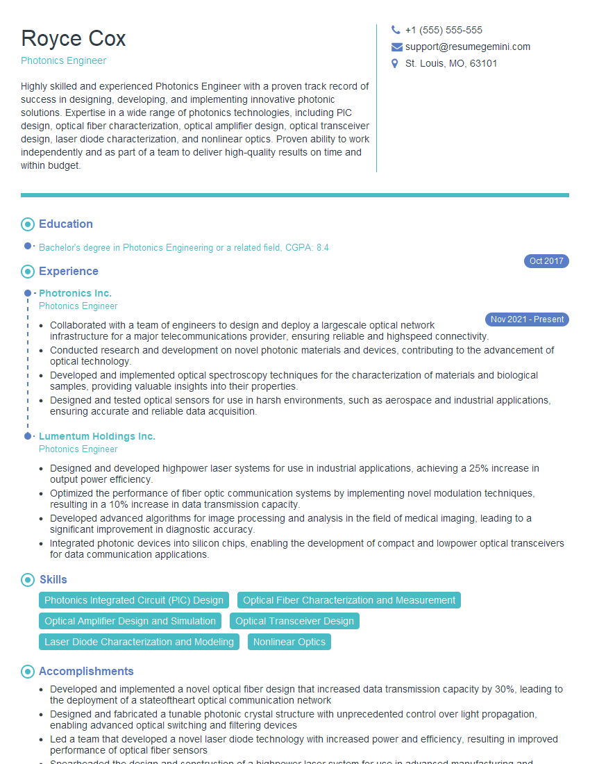
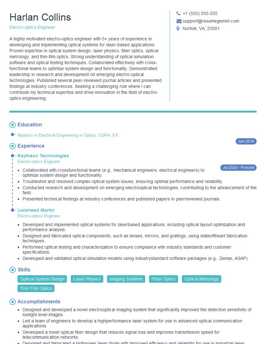
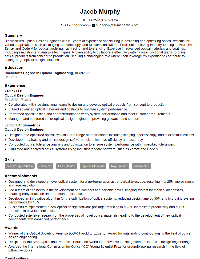
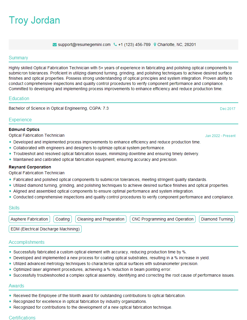
Mastering Advanced Optics Manufacturing (AOM) training opens doors to exciting and rewarding careers in a cutting-edge field. To maximize your job prospects, a well-crafted resume is essential. An ATS-friendly resume increases your chances of getting noticed by recruiters and securing interviews. We strongly recommend using ResumeGemini, a trusted resource, to build a professional and impactful resume. ResumeGemini provides examples of resumes specifically tailored to Advanced Optics Manufacturing (AOM) training to help guide you. Invest the time to create a compelling resume—it’s a significant step in your journey towards a successful career in AOM.
Explore more articles
Users Rating of Our Blogs
Share Your Experience
We value your feedback! Please rate our content and share your thoughts (optional).
What Readers Say About Our Blog
Interesting Article, I liked the depth of knowledge you’ve shared.
Helpful, thanks for sharing.
Hi, I represent a social media marketing agency and liked your blog
Hi, I represent an SEO company that specialises in getting you AI citations and higher rankings on Google. I’d like to offer you a 100% free SEO audit for your website. Would you be interested?
