Preparation is the key to success in any interview. In this post, we’ll explore crucial Schematic and Panel Layout Design interview questions and equip you with strategies to craft impactful answers. Whether you’re a beginner or a pro, these tips will elevate your preparation.
Questions Asked in Schematic and Panel Layout Design Interview
Q 1. Explain the difference between a schematic and a PCB layout.
A schematic and a PCB layout are two distinct but interconnected stages in the design of a printed circuit board (PCB). Think of the schematic as the blueprint of your electronic circuit, a high-level representation showing the components and their connections. The PCB layout, on the other hand, is the physical manifestation of that blueprint—it’s the detailed plan specifying the exact placement of components and the routing of traces on the PCB itself.
The schematic uses symbols to represent components and lines to represent connections, focusing on functionality and connectivity. It doesn’t specify physical dimensions or component locations. In contrast, the PCB layout is a detailed 2D or 3D representation showing the actual physical placement of components on the board, the widths and lengths of traces, the layers, and other manufacturing details. You can think of it as the architectural plan translating the initial concept into a buildable structure.
For example, a schematic might show a resistor connected to a capacitor and a microcontroller. The PCB layout would then define the exact coordinates of each of these components on the board and the specific paths the traces will take to connect them, considering factors like trace width, layer assignment, and proximity to other components.
Q 2. Describe your experience with different PCB layout software (e.g., Altium, Eagle, KiCad).
Throughout my career, I’ve extensively used Altium Designer, Eagle, and KiCad, each with its own strengths and weaknesses. Altium Designer is a powerful, industry-standard software with advanced features for high-speed design, excellent library management, and robust design rule checking. I’ve used it on projects involving complex multi-layer boards with stringent signal integrity requirements. Eagle, while simpler and perhaps easier to learn initially, is suitable for smaller, less complex projects. Its ease of use makes it great for rapid prototyping.
KiCad, a free and open-source option, has become increasingly sophisticated. I’ve found it particularly useful for projects where budget is a constraint. While its interface might not be as polished as Altium’s, its capabilities are quite impressive, especially in recent versions. The ability to customize and extend its functionality with scripting makes it highly versatile.
My selection of software depends heavily on the project’s complexity, budget, and timeline. For instance, a high-speed, high-density design would necessitate the power of Altium, whereas a quick prototype might be best tackled with Eagle. KiCad is an excellent alternative for projects where cost is a major factor without compromising on design quality.
Q 3. How do you handle high-speed signal routing in PCB design?
High-speed signal routing demands meticulous attention to detail. The goal is to minimize signal reflections, crosstalk, and electromagnetic interference (EMI). My approach involves several key strategies:
- Controlled Impedance Routing: I carefully define and maintain consistent trace impedance throughout the high-speed signal paths. This requires selecting the appropriate trace width, spacing, and layer stackup to achieve the desired impedance. Tools within the PCB layout software help calculate and verify impedance.
- Minimizing Trace Lengths: Shorter traces reduce signal propagation delays and the risk of reflections. Careful placement of components and strategic routing are crucial here.
- Differential Pair Routing: For differential signals, I maintain consistent trace lengths and spacing between the two conductors, ensuring they are routed in close proximity and symmetrically to minimize EMI and crosstalk.
- Proper Termination: Terminating the high-speed signals at the source and destination with appropriate resistors (e.g., series termination, parallel termination) helps prevent reflections and ensures signal integrity. The choice of termination depends on the specific system requirements.
- Avoid sharp bends and vias: Sharp bends and vias can introduce unwanted impedance discontinuities, which can cause signal reflections. I strive for smooth, gentle curves and minimize vias along high-speed signal traces.
For instance, in designing a high-speed data acquisition system, adhering to these principles is critical to maintain data accuracy. Neglecting these aspects can lead to signal degradation, data loss, and system malfunction.
Q 4. What are your strategies for managing component placement and thermal considerations?
Component placement and thermal management are deeply intertwined. My strategies focus on optimizing both simultaneously:
- Thermal Vias: For power components that generate significant heat, I use thermal vias to efficiently transfer heat away from the component to the PCB’s copper planes or to a heat sink. The number and placement of these vias are crucial for effective heat dissipation.
- Heat Sink Integration: For high-power applications, I integrate heat sinks into the design, ensuring adequate thermal contact between the component and the heat sink. This requires careful consideration of the heat sink’s size, material, and attachment mechanism.
- Component Spacing: Sufficient spacing between components is crucial to prevent overheating. This is particularly important for high-power components. I use the software’s thermal simulation capabilities to verify temperatures.
- Airflow Considerations: For high-power systems, I consider airflow pathways to facilitate natural or forced-air cooling. This often involves strategic component placement to maximize airflow around heat-generating components.
- Placement for Signal Integrity: Component placement is also governed by signal integrity considerations. For instance, sensitive analog components should be placed far away from noisy digital components. Balancing thermal and signal integrity requirements is essential.
Imagine designing a power supply; incorrect placement can lead to overheating and premature component failure. Therefore, thermal simulation and careful planning are key in creating a reliable design.
Q 5. Explain your process for creating a robust and manufacturable PCB design.
Creating a manufacturable PCB design requires a systematic approach:
- Design Rules Checking (DRC): Thorough DRC is paramount to catch design violations early. This involves setting design rules based on the chosen manufacturing process and verifying that the layout complies with these rules. The software will highlight any potential issues, such as trace clearances, via sizes, and pad sizes.
- Design for Manufacturing (DFM): DFM analysis considers the limitations and capabilities of the chosen manufacturing process. It ensures that the design is feasible to manufacture and avoids features that are difficult or impossible to fabricate. This might include considering the minimum trace width, minimum hole size, and board dimensions.
- Gerber File Generation: After completing the layout, generating accurate Gerber files is crucial. These files contain the manufacturing information needed by the PCB fabricator. Careful verification of these files is essential to avoid errors.
- Component Selection: Choosing components that are readily available and compatible with the chosen manufacturing process is important. It’s best to select components with industry-standard packages.
- Documentation: Comprehensive documentation, including a bill of materials (BOM), schematic, and design specifications, is essential for easy replication and future maintenance.
A well-documented and thoroughly checked PCB design drastically reduces manufacturing errors and significantly lowers production costs and turnaround time. Overlooking these steps leads to potentially expensive revisions and delays.
Q 6. How do you ensure signal integrity in your designs?
Ensuring signal integrity requires a multi-faceted approach beginning even before the layout stage:
- Careful Component Selection: Choosing components with appropriate specifications for the targeted frequency range is paramount. For high-speed applications, selecting components with low parasitic capacitance and inductance is critical.
- Proper Grounding and Power Planes: Establishing a robust ground plane and distributing power efficiently are essential. Multiple ground planes might be necessary for complex designs to minimize noise coupling.
- Controlled Impedance Routing (as mentioned earlier): Maintaining consistent impedance is crucial for high-speed signals to prevent reflections and signal degradation.
- Crosstalk Mitigation: Careful routing to minimize the proximity between sensitive signals and high-speed traces helps to avoid crosstalk. This includes utilizing shielding, differential signaling, and guard traces.
- Simulation and Analysis: Utilizing simulation tools (e.g., IBIS-AMI, SPICE) to analyze signal integrity is an invaluable step. This allows for identifying potential problems before manufacturing.
Imagine designing a high-speed communication link—without careful consideration of signal integrity, errors and data corruption could result. Simulation helps identify and correct those issues early in the design process, before significant resources are invested.
Q 7. Describe your experience with different PCB fabrication processes.
I have experience with various PCB fabrication processes, including:
- Additive Processes: These processes build the PCB layer by layer, such as inkjet printing or laser ablation. They are suitable for rapid prototyping and low-volume production.
- Subtractive Processes: These processes start with a base material (e.g., copper-clad laminate) and remove unwanted material to create the PCB traces and pads. This is the most common method for mass production.
- Different Laminates and Materials: I’m familiar with different types of laminates and materials, such as FR-4, high-Tg materials, and flexible PCBs, each with different properties suitable for specific applications and requirements.
- Surface Finishes: Understanding various surface finishes (e.g., HASL, ENIG, OSP) and their impact on solderability and reliability is crucial. The choice of finish depends on the application and cost constraints.
For instance, high-frequency applications might require a specific laminate material with low dielectric loss, while a high-temperature application might demand a high-Tg material. Choosing the right materials and processes is key to a successful product.
Q 8. How do you manage design changes and revisions?
Managing design changes and revisions effectively is crucial for successful PCB design. My approach centers around a robust version control system, typically Git, integrated with a schematic capture and PCB layout tool. Each revision is clearly documented with a change log detailing the modifications, the reason behind them, and the impact on the overall design. This ensures traceability and allows for easy rollback if needed.
For example, if a component needs to be replaced, I’ll create a new revision, updating the schematic and layout, documenting the old and new component details, and highlighting any necessary routing changes. The version control system provides a clear history, allowing us to compare different revisions side-by-side and easily identify the source of any issues. We also use a formal review process where colleagues inspect design changes before they are implemented, catching potential problems early. This collaborative approach, coupled with a well-defined change management process, helps prevent conflicts and ensures design integrity.
Q 9. Explain your understanding of impedance matching and its importance in PCB design.
Impedance matching is the practice of ensuring that the impedance of different parts of a circuit are properly matched to minimize signal reflections and maximize power transfer. In PCB design, this is particularly important for high-speed signals, such as those used in digital communication and high-frequency applications. Mismatched impedance can lead to signal degradation, noise, and ultimately system malfunction.
Imagine sending a wave down a rope; if the rope suddenly changes thickness, the wave will partially reflect back. Similarly, if a signal encounters a significant impedance mismatch on a PCB trace, a portion of the signal reflects back towards the source, creating signal distortion and potentially interfering with other signals. I ensure impedance matching by using controlled impedance trace widths and lengths, carefully selecting materials, and using impedance-matched connectors. Tools like simulation software are used to verify the impedance profile of the PCB before manufacturing.
Q 10. How do you handle EMI/EMC compliance in your designs?
Handling EMI/EMC compliance is a critical aspect of PCB design, ensuring that the device doesn’t emit excessive electromagnetic interference (EMI) or is susceptible to electromagnetic susceptibility (EMS). My approach involves a multi-pronged strategy starting early in the design process.
This begins with careful component selection, favoring components with low EMI emission. I strategically place and route components, keeping high-speed signals away from sensitive analog circuits and using appropriate shielding techniques like ground planes and conductive enclosures. Furthermore, I incorporate filtering components, like ferrite beads and capacitors, to suppress unwanted noise. Post-layout, I use simulation tools to predict EMI/EMC performance, and physical measurements are performed on prototypes to ensure compliance with standards like CISPR and FCC regulations. Any necessary adjustments are made iteratively, ensuring the final product meets the required standards.
Q 11. Describe your experience with design rule checking (DRC) and its significance.
Design rule checking (DRC) is an automated process that verifies the PCB layout against a set of predefined rules. These rules ensure that the design is manufacturable and meets specific electrical and physical requirements. DRC is an essential part of my workflow, catching errors early in the design process, preventing costly rework later.
For example, DRC checks for clearance violations between traces, minimum trace widths, proper pad sizes, and other critical parameters. By running DRC checks regularly throughout the design process, I identify and correct errors quickly. I typically use the built-in DRC engine of my PCB design software, customizing the rules to match the specific requirements of the manufacturing process and the application. Failing a DRC check is a significant issue, indicating potential manufacturability problems, so addressing the flagged errors is crucial before proceeding to fabrication.
Q 12. How do you ensure your designs meet regulatory standards (e.g., UL, CE)?
Meeting regulatory standards like UL and CE is paramount for ensuring product safety and market access. My process involves meticulous adherence to the relevant standards throughout the design process. This includes selecting components with appropriate certifications, following specific layout guidelines related to safety clearances and isolation, and implementing robust power supply design practices.
Specific to UL standards, I pay close attention to creepage and clearance distances, ensuring appropriate insulation between live parts and ground. For CE compliance, I rigorously test the device’s emissions and immunity against electromagnetic disturbances. Thorough documentation of the design process, including component selection, test results, and compliance verification, is crucial to demonstrate adherence to these standards. I work closely with testing labs when necessary, conducting rigorous testing to ensure that the final product meets all relevant standards before launching the product.
Q 13. What are your preferred methods for PCB design verification and validation?
PCB design verification and validation are critical steps to guarantee a functional and reliable product. My preferred methods combine simulation and physical testing.
Simulation involves using tools to model the behavior of the circuit under various conditions. This helps identify potential issues early in the design process, before the board is manufactured. I use tools to simulate signal integrity, power integrity, and thermal performance. Physical testing involves building prototypes and conducting various tests, such as functional testing, thermal cycling, and environmental stress tests, to validate the design’s performance under real-world conditions. A combination of these approaches gives me a high degree of confidence in the final design’s reliability and functionality.
Q 14. Describe your experience with component libraries and their management.
Component libraries are essential for efficient PCB design. I maintain well-organized libraries, ensuring that each component has accurate specifications and footprints. This requires a systematic approach to managing the library, ensuring that all parts are up-to-date and accurately modeled.
I use a combination of manufacturer-supplied libraries and my own custom-created libraries. For custom components, I meticulously verify the 3D models and footprints for accuracy to prevent mismatches or design errors. Regular updates and version control for the libraries are important to ensure data integrity and avoid compatibility problems. A well-organized library saves time, reduces errors, and improves design consistency across projects.
Q 15. How do you manage layer stackups in PCB design?
Layer stackup in PCB design refers to the vertical arrangement of different conductive and insulating layers. Think of it like a layered cake, where each layer has a specific purpose. Effective layer stackup is crucial for signal integrity, impedance control, and overall PCB performance.
Managing it involves careful consideration of several factors:
- Signal Layers: These carry high-speed signals and require meticulous planning to minimize crosstalk and ensure signal integrity. The number of signal layers depends on the complexity of the design.
- Power/Ground Planes: Solid copper planes are essential for reducing noise, distributing power evenly, and providing a return path for signals. Their placement is strategic to minimize impedance and improve signal quality. For example, a common arrangement is to have a power plane and a ground plane adjacent to signal layers.
- Internal Plane Layers: These can be used for power or ground distribution, especially in high-layer-count boards. They aid in reducing noise and improving signal integrity.
- Prepreg Layers: These are insulating layers between conductive layers, critical for mechanical support and electrical insulation. The choice of prepreg material impacts the overall impedance and thermal performance.
- Substrate Material: The base material of the PCB (e.g., FR4, Rogers) greatly affects the overall properties of the stackup, influencing dielectric constant, dissipation factor, and thermal conductivity.
I typically use PCB design software to model the layer stackup, simulating impedance and other parameters to ensure optimal performance. For instance, I might use a simulator to check that the trace impedance aligns with the specifications required for high-speed signals, and adjust the layer stackup if necessary.
Career Expert Tips:
- Ace those interviews! Prepare effectively by reviewing the Top 50 Most Common Interview Questions on ResumeGemini.
- Navigate your job search with confidence! Explore a wide range of Career Tips on ResumeGemini. Learn about common challenges and recommendations to overcome them.
- Craft the perfect resume! Master the Art of Resume Writing with ResumeGemini’s guide. Showcase your unique qualifications and achievements effectively.
- Don’t miss out on holiday savings! Build your dream resume with ResumeGemini’s ATS optimized templates.
Q 16. What are your preferred techniques for trace routing?
Trace routing is the process of connecting components on a PCB using conductive traces. My preferred techniques prioritize signal integrity, manufacturability, and design for testability. These include:
- Automated Routing: I leverage the automated routing features of my PCB design software as a starting point. This provides a quick initial solution that I can then refine manually.
- Manual Routing: For critical high-speed signals or areas with high component density, I perform manual routing for precise control. This allows me to optimize trace length, minimize vias (connection points between layers), and control impedance.
- Differential Pair Routing: For sensitive analog or high-speed digital signals, I use differential pair routing, ensuring controlled impedance and equal trace length for both signals in the pair, thus minimizing electromagnetic interference (EMI).
- Constraint-Driven Routing: I define routing constraints, such as trace width, length, impedance, and spacing, to meet signal integrity requirements. This is especially important for high-speed designs.
- Layer Assignment Strategies: I carefully assign traces to specific layers based on signal characteristics and layer stackup. For instance, critical high-speed signals might be assigned to inner layers for better noise immunity.
For example, when routing high-speed differential pairs, I ensure the traces are closely spaced, have controlled impedance, and are of equal length to minimize crosstalk and maintain signal integrity. I also document routing decisions for future reference.
Q 17. How do you handle complex signal routing challenges?
Complex signal routing challenges often arise in high-density designs with high-speed signals and tight constraints. My approach involves a systematic strategy:
- Careful Planning and Design Review: Before starting the routing process, I thoroughly review the schematic, considering signal integrity requirements and potential challenges.
- Constraint Definition: I rigorously define routing constraints based on signal characteristics (e.g., rise/fall time, frequency) and manufacturing tolerances.
- Multilayer Stackup Optimization: I optimize the layer stackup to minimize crosstalk and ensure optimal impedance control.
- Smart Via Placement: I strategically place vias to minimize parasitic inductance and capacitance and maintain signal integrity. I avoid unnecessary vias.
- Iterative Routing and Simulation: I use simulation tools to verify signal integrity, analyzing parameters like eye diagrams and jitter. This allows for iterative refinements of the routing to optimize performance.
- Use of Specialized Routing Techniques: Depending on the specific challenge, I may employ advanced techniques like controlled impedance routing, differential pair routing, or shielding for sensitive signals.
For instance, in a recent project with many high-speed serial links, I had to use controlled impedance routing and differential pair routing to meet the stringent timing requirements. Simulation was crucial to identify and resolve signal integrity issues before manufacturing.
Q 18. What are your strategies for minimizing power consumption in PCB designs?
Minimizing power consumption in PCB designs is crucial for extending battery life, reducing heat dissipation, and improving overall efficiency. My strategies include:
- Component Selection: I choose low-power components whenever possible, comparing datasheets for power consumption figures.
- Power Supply Design: I carefully design the power supply, employing efficient switching regulators and minimizing voltage drops.
- Power Plane Design: Effective power plane design reduces voltage fluctuations and improves overall efficiency.
- Trace Routing Optimization: Minimizing trace lengths reduces resistance, and thus power loss.
- Efficient Switching Strategies: I use efficient switching techniques for digital circuits to reduce power consumption during idle periods. Low power modes of components should be considered.
- Thermal Management: Proper thermal management solutions such as heat sinks can improve efficiency and reduce power losses due to heating.
For example, I once worked on a battery-powered device where careful component selection and power supply optimization led to a 20% reduction in power consumption compared to the initial design.
Q 19. Explain your experience with simulation tools for PCB design.
I have extensive experience using simulation tools such as Altium Designer’s built-in simulators, HyperLynx, and Sigrity. These tools are invaluable for predicting PCB behavior and resolving potential problems early in the design cycle.
My use of simulation tools involves:
- Signal Integrity Analysis: I use simulators to analyze signal integrity, identifying potential issues such as reflections, crosstalk, and impedance mismatch.
- Power Integrity Analysis: I employ power integrity analysis to identify potential voltage drops, noise issues, and other power-related concerns.
- Thermal Analysis: Thermal simulation helps predict temperature distributions on the PCB, allowing for optimization of heat dissipation strategies.
- EMI/EMC Analysis: I use simulation to analyze EMI/EMC compliance, identifying potential sources of interference and implementing solutions.
For example, during a high-speed design, using HyperLynx, I was able to identify and correct a significant impedance mismatch before manufacturing, saving time and resources.
Q 20. How do you collaborate with other engineers and stakeholders during the design process?
Collaboration is key in PCB design. I leverage various methods to effectively communicate and work with other engineers and stakeholders:
- Clear Communication: I ensure clear and concise communication through regular meetings, email updates, and shared design documents. I use visual aids such as schematics and layouts to illustrate technical points.
- Version Control: I use version control systems to manage design files, track changes, and facilitate collaboration among team members. This allows for easy rollback if needed.
- Design Reviews: Regular design reviews involve presenting the design to peers and stakeholders, gathering feedback, and addressing concerns.
- Tool Usage: Utilizing collaborative design platforms allows for real-time co-editing and feedback.
- Documentation: Meticulous documentation of design decisions and rationale is critical for maintaining transparency and understanding.
For instance, in a recent project, using a shared online platform, I worked closely with the mechanical engineer to ensure that the PCB design was compatible with the enclosure.
Q 21. What are some common PCB design errors and how to avoid them?
Common PCB design errors can lead to costly rework and delays. Some frequent ones include:
- Incorrect Component Placement: Poor component placement can lead to routing difficulties and signal integrity issues. Careful planning is crucial.
- Insufficient Clearance: Inadequate clearance between traces and components can result in shorts and malfunctions. Design rules checking (DRC) is vital.
- Uncontrolled Impedance: Not managing impedance, especially for high-speed signals, results in signal degradation and performance issues.
- Improper Grounding: Poor grounding practices can lead to noise problems and signal integrity issues. Careful attention to ground planes and connections is necessary.
- Lack of Thermal Management: Failure to account for heat dissipation can damage components and lead to system failure.
- Ignoring Design Rules: Neglecting to follow design rules leads to manufacturing issues and unexpected problems.
To avoid these errors, I rigorously adhere to design rules, use simulation tools for verification, conduct thorough design reviews, and meticulously check the design using automated DRC and LVS (Layout Versus Schematic) tools before proceeding to manufacturing.
Q 22. How do you handle design constraints and trade-offs?
Handling design constraints and trade-offs is a crucial aspect of PCB design. It’s like balancing a complex equation where every component has a weight and influence. We’re constantly navigating between competing requirements such as size, cost, performance, and thermal management. For instance, using a smaller, cheaper capacitor might save money, but it could compromise performance or introduce stability issues. My approach involves a structured process:
- Clearly Defining Requirements: Starting with a thorough understanding of the project’s specifications and priorities is paramount. This involves close collaboration with the client or engineering team.
- Prioritization and Ranking: Once the requirements are listed, we rank them based on importance. This might involve assigning weights or using a decision matrix. Some features are non-negotiable, others can be compromised if necessary.
- Trade-off Analysis: We systematically evaluate the impact of different design choices on each requirement. This often involves using simulation tools to model performance and identify potential bottlenecks.
- Iteration and Refinement: The initial design is rarely perfect. We iterate on the design, making adjustments and re-evaluating the trade-offs until an optimal balance is achieved.
- Documentation: All design decisions, including the trade-offs made, are meticulously documented to ensure transparency and facilitate future modifications.
For example, in a recent project with strict size constraints, we had to choose between using a surface-mount technology (SMT) component or a through-hole component. While through-hole components offer greater robustness, their larger size conflicted with the space limitations. Opting for SMT components, despite a slight increase in cost and potential for higher manufacturing complexity, ultimately allowed us to meet the size requirements without compromising functionality.
Q 23. Describe your experience with different types of connectors and their applications.
My experience encompasses a wide range of connectors, each with its specific advantages and disadvantages. The choice of connector depends heavily on the application’s requirements, including signal integrity, power handling, environmental conditions, and cost.
- High-Speed Connectors: For high-speed digital applications, such as those found in server boards or high-end networking equipment, specialized connectors like Samtec, TE Connectivity, or Amphenol are critical for minimizing signal loss and impedance mismatches. These often involve careful considerations of connector placement and routing to ensure signal integrity.
- Power Connectors: Handling significant power requires robust connectors with appropriate current ratings and contact configurations. These might include screw-terminal blocks for higher currents or specialized power connectors for higher voltage applications. Proper thermal management is vital with these connectors to avoid overheating.
- Board-to-Board Connectors: These range from simple headers and sockets for low-speed applications to high-density connectors for dense packaging. Careful selection is crucial to ensure sufficient mating cycles and durability.
- I/O Connectors: Connectors such as USB, Ethernet, or HDMI, each come with their own specifications for signal transmission and mechanical interface. These necessitate adherence to industry standards and careful design for proper signal integrity.
- Specialty Connectors: Applications often demand specialized connectors like circular connectors for harsh environmental conditions or fiber optic connectors for high-bandwidth communication.
In one project, selecting the right USB-C connector was crucial for achieving the desired data transfer rates and power delivery capabilities. We carefully evaluated different connector options, comparing their bandwidth, power handling capacity, and mechanical robustness, before settling on a connector that met the application’s stringent requirements.
Q 24. How do you document your PCB designs effectively?
Effective documentation is paramount for successful PCB design and subsequent manufacturing and maintenance. Think of it as a roadmap for the entire project lifecycle. My approach emphasizes clarity, completeness, and accessibility.
- Schematic Documentation: This includes a well-organized schematic with clear naming conventions, component annotations, and design notes. We use version control to track changes and ensure everyone works from the latest version.
- PCB Layout Documentation: This involves clear layer designations, a well-documented bill of materials (BOM), and detailed fabrication drawings. We also maintain a comprehensive design rule check (DRC) report to ensure manufacturability.
- Gerber Files and Fabrication Drawings: These are the cornerstone of manufacturing. We carefully generate and verify these files, ensuring they accurately reflect the final design.
- Assembly Drawings and Instructions: Detailed assembly drawings make it easier to understand how the PCB fits within the larger system. These are especially crucial for complex designs.
- Design Reviews and Sign-offs: Formal design reviews are essential for validating the design and resolving potential issues before proceeding to fabrication.
For example, our documentation also includes detailed notes explaining critical design decisions, such as component selection rationale, thermal considerations, and signal integrity analysis. This ensures maintainability, even years after the product’s launch.
Q 25. What are your strategies for debugging PCB design issues?
Debugging PCB design issues can be like detective work, requiring a systematic approach and the right tools. I employ a multi-stage strategy:
- Initial Assessment: This involves reviewing the design documentation and performing visual inspections to identify any obvious errors or inconsistencies.
- Simulation and Analysis: Simulation tools are indispensable for analyzing signals and identifying potential issues. We use signal integrity analysis, power integrity analysis, and thermal analysis to diagnose issues before fabrication.
- In-Circuit Testing (ICT): ICT helps verify component connectivity and identify open or shorted circuits early in the testing process.
- Functional Testing: Once the PCB is assembled, functional tests are performed to verify the operation of the circuit under various conditions.
- Logic Analyzers and Oscilloscopes: These tools provide invaluable insights into signal behavior, allowing for the identification of timing issues, signal noise, or other anomalies.
- Debugging Techniques: We use techniques such as probing key nodes with oscilloscopes, inserting test points, and using current probes to isolate faulty components or connections.
In a past project, an intermittent power failure plagued the system. By utilizing an oscilloscope, we discovered that the issue stemmed from insufficient decoupling capacitance on the power supply lines. Adding additional capacitors resolved the problem.
Q 26. Explain your experience with manufacturing process optimization for PCB designs.
Manufacturing process optimization is crucial for reducing costs, improving quality, and shortening lead times. My experience in this area focuses on understanding the manufacturing process intimately and working closely with the fabricators.
- Design for Manufacturing (DFM): We prioritize DFM principles during the design process, ensuring the design is manufacturable and cost-effective. This includes using standard component sizes and packages, optimizing trace routing for manufacturability, and avoiding complex geometries.
- Collaboration with Fabricators: Early and frequent communication with fabricators is critical for understanding their capabilities and constraints. We involve them early in the design process to ensure manufacturability and identify potential issues upfront.
- Material Selection: The choice of PCB materials directly affects the manufacturing process and final product cost. Selecting appropriate materials with respect to the application’s requirements is key to optimization.
- Component Selection: Using readily available and cost-effective components minimizes procurement lead times and reduces overall costs.
- Testing and Feedback: Working closely with the fabricator to test and refine the manufacturing process leads to improvements in yield and reduces scrap.
In one project, by carefully selecting more readily available components and simplifying the PCB layout, we managed to decrease the manufacturing cost by 15% and reduce the lead time by 10 days.
Q 27. How do you stay updated with the latest advancements in PCB design technology?
Staying current in PCB design technology is an ongoing process. I employ several strategies to keep my skills sharp and knowledge up-to-date.
- Industry Publications and Conferences: I regularly read industry publications like Electronics Weekly, EDN, and Circuit Cellar. Attending conferences and workshops allows me to learn about the latest tools and techniques.
- Online Resources and Courses: Online resources such as webinars, tutorials, and online courses on platforms like Coursera and edX provide in-depth knowledge on specific technologies.
- Professional Organizations: Being a member of professional organizations such as IPC (Association Connecting Electronics Industries) keeps me informed about the latest standards and best practices.
- Collaboration and Networking: Regularly interacting with peers, attending industry events, and participating in online forums allows for knowledge exchange and staying abreast of emerging technologies.
- Hands-on Experience: There’s no substitute for hands-on experience. I actively seek opportunities to work on projects that utilize the latest technologies and techniques.
For example, recently I completed a course on high-speed digital design, focusing on techniques for minimizing signal integrity issues in high-speed applications. This directly improved my skillset for upcoming projects.
Q 28. Describe a challenging PCB design project you worked on and how you overcame the challenges.
One particularly challenging project involved designing a high-speed, high-density PCB for a medical imaging system. The primary challenges included stringent signal integrity requirements, tight space constraints, and rigorous EMC/EMI regulations.
Overcoming these challenges required a multi-pronged approach:
- Signal Integrity Analysis: We used advanced simulation tools to model signal propagation and identify potential issues like reflections and crosstalk. This involved meticulous routing and careful component placement.
- EMI/EMC Compliance: To meet strict regulations, we implemented various techniques such as proper grounding, shielding, and filtering. This required a deep understanding of EMI/EMC principles and the use of specialized simulation tools.
- Thermal Management: The high power consumption of the system necessitated careful thermal management to prevent overheating. This involved strategic placement of heat sinks and careful routing of power traces.
- Iterative Design Process: We utilized an iterative design process, constantly refining the design based on simulation results and prototype testing. This involved numerous revisions and close collaboration with the engineering team.
The successful completion of this project demonstrated our ability to overcome complex design constraints while adhering to stringent industry regulations and performance requirements. The lessons learned from this project have significantly enhanced our team’s capabilities in handling future high-speed, high-density designs.
Key Topics to Learn for Schematic and Panel Layout Design Interview
- Schematic Capture & Design Principles: Understanding fundamental schematic design principles, including component placement, netlisting, and hierarchical design methodologies. Practical application: Designing a schematic for a simple circuit and explaining your design choices.
- Component Selection & Datasheet Interpretation: Selecting appropriate components based on specifications and interpreting datasheets to understand component limitations and capabilities. Practical application: Justifying component choices in a given design scenario.
- PCB Layout Techniques: Mastering routing techniques (e.g., auto-routing, manual routing), signal integrity considerations, and power distribution design. Practical application: Discussing strategies for minimizing EMI and signal crosstalk.
- Design Rule Checking (DRC) & Electrical Rule Checking (ERC): Understanding and utilizing DRC and ERC tools to identify and resolve design errors before fabrication. Practical application: Explaining the importance of thorough design checks and their impact on product reliability.
- Manufacturing Considerations: Understanding the impact of design choices on manufacturability, including DFM (Design for Manufacturing) and DFA (Design for Assembly). Practical application: Discussing design modifications to improve manufacturability.
- Software Proficiency: Demonstrating familiarity with industry-standard schematic capture and PCB layout software (e.g., Altium Designer, Eagle, KiCad). Practical application: Describing your experience with specific software features and workflows.
- Simulation and Analysis: Utilizing simulation tools to verify circuit functionality and identify potential issues before prototyping. Practical application: Explaining the types of simulations you’ve used and the insights gained.
Next Steps
Mastering Schematic and Panel Layout Design is crucial for a successful career in electronics engineering, offering exciting opportunities in diverse industries. A strong understanding of these principles significantly enhances your problem-solving abilities and allows you to contribute meaningfully to innovative projects. To maximize your job prospects, it’s vital to craft an ATS-friendly resume that effectively showcases your skills and experience. ResumeGemini is a trusted resource to help you build a professional and impactful resume. Take advantage of their tools and resources; examples of resumes tailored specifically to Schematic and Panel Layout Design are available to help you get started.
Chief Engineer Resume Sample
Engineering Manager Resume Sample

Project Engineer Resume Sample
Systems Engineer Resume Sample
Applications Engineer Resume Sample
Test Engineer Resume Sample
Design Engineer Resume Sample
Hardware Design Engineer Resume Sample
Senior Hardware Engineer Resume Sample
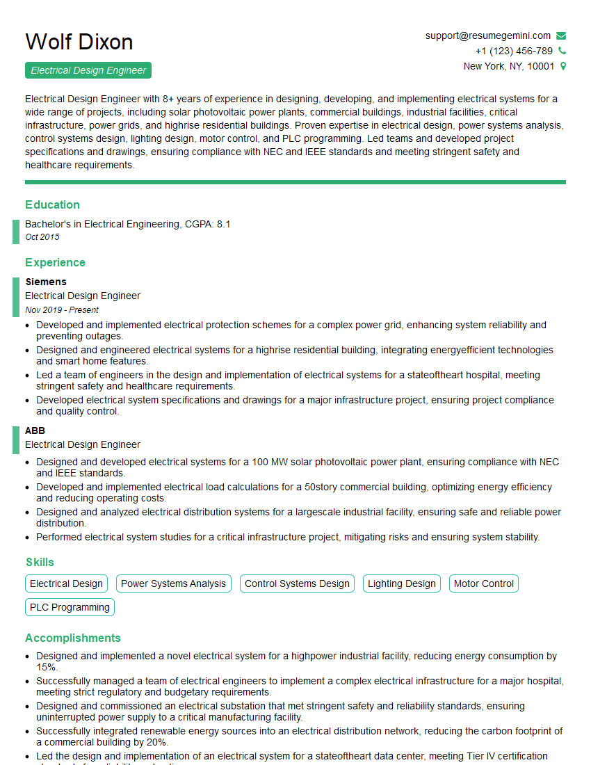
Electrical Design Engineer Resume Sample
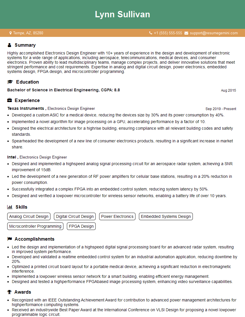
Electronics Design Engineer Resume Sample
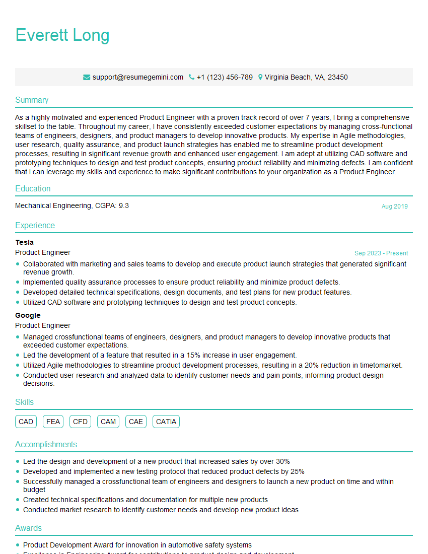
Product Engineer Resume Sample
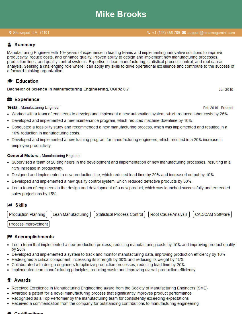
Manufacturing Engineer Resume Sample
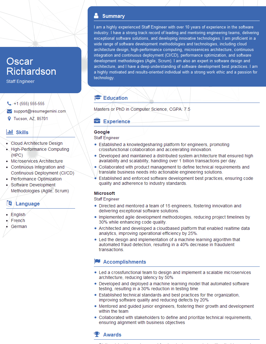
Staff Engineer Resume Sample
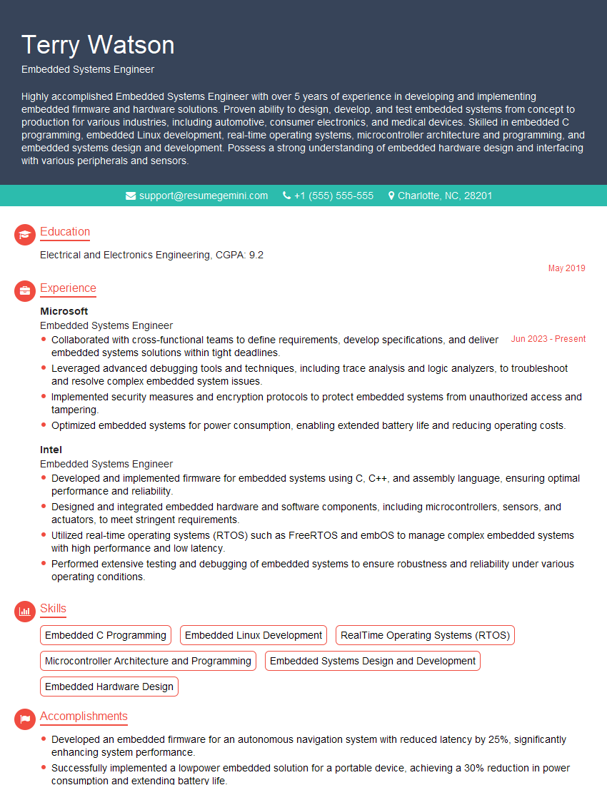
Embedded Systems Engineer Resume Sample
- Chief Engineer
- Engineering Manager
- Project Engineer
- Systems Engineer
- Applications Engineer
- Test Engineer
- Design Engineer
- Hardware Design Engineer
- Senior Hardware Engineer
- Electrical Design Engineer
- Electronics Design Engineer
- Product Engineer
- Manufacturing Engineer
- Staff Engineer
- Embedded Systems Engineer
Explore more articles
Users Rating of Our Blogs
Share Your Experience
We value your feedback! Please rate our content and share your thoughts (optional).
What Readers Say About Our Blog
Amazing blog
Interesting Article, I liked the depth of knowledge you’ve shared.
Helpful, thanks for sharing.